
More Information
Submitted: April 03, 2025 | Approved: April 15, 2025 | Published: April 16, 2025
How to cite this article: Alaskari MKG, Sepehri A, Kassaee MZ. Unlocking Graphene’s Potential: Size Distribution and Topological Advances. Int J Phys Res Appl. 2025; 8(4): 052-058. Available from:
https://dx.doi.org/10.29328/journal.ijpra.1001115
DOI: 10.29328/journal.ijpra.1001115
Copyright license: © 2025 Alaskari MKG, et al. This is an open access article distributed under the Creative Commons Attribution License, which permits unrestricted use, distribution, and reproduction in any medium, provided the original work is properly cited.
Keywords: Field emission scanning electron microscopy (FESEM), Fourier-transform infrared (FT-IR), Graphene, Graphene Oxide (GO), Nanomaterial, Twisted Multilayers, UV-Visible Spectroscopy, X-ray diffraction (XRD)

Unlocking Graphene’s Potential: Size Distribution and Topological Advances
Mohammad Kamal Ghassem Alaskari1*, Amir Sepehri2 and Mohammad Zaman Kassaee3
1Department of Petroleum Engineering, Petroleum University of Technology, Tehran, Iran
3Department of Petroleum Engineering, Islamic Azad University Science and Research Branch, Tehran, Iran
3Department of Chemistry, Tarbiat Modares University, Tehran, Iran
*Address for Correspondence: Mohammad Kamal Ghassem Alaskari, Department of Petroleum Engineering, Petroleum University of Technology, Tehran, Iran, Email: [email protected]
The size distribution and topological properties of graphene samples in two-dimensional (2D) sheets play a crucial role in various technological applications and can be characterized using multiple analytical techniques, including X-ray diffraction (XRD), Field-Emission Scanning Electron Microscopy (FESEM), Fourier-transform infrared spectroscopy (FT-IR), UV-visible spectroscopy (UV-vis), and Raman spectroscopy. In this study, we investigated the size distribution and topological features of hexagonal twisted graphene sheets and their impact on band gap energy, utilizing first-principles calculations based on Bragg's law and the Scherrer equation. Our findings demonstrate that the band gap topology of graphene sheets can be effectively modulated by introducing twisted multilayer graphene configurations.
Furthermore, the incorporation of spin-orbit coupling induces a two-band gap structure in bilayer graphene, particularly at n = 1/3 in the quantum Hall regime, significantly enhancing the potential energy of charge carriers. The measured band gaps are as follows:
- Graphene nanocrystals (GNs): 2.12 eV
- Partially reduced graphene oxide (PRGO): 0.3 – 1.5 eV
- Graphene Oxide (GO): 2.1 – 3.5 eV
Additional analyses indicate that these findings hold significant promise for the development of Field-Effect Transistors (FETs) and quantum-state superconductors, which are essential components in emerging quantum devices, including medical MRI systems, quantum computing architectures, and quantum memory storage.
Carbon is a remarkably strong element, and its allotrope, graphite, also exhibits significant strength. Graphene's application in radiation shielding has shown considerable promise, enhancing the efficiency and practicality for electromagnetic shielding technologies such as antennas and enclosures. Electromagnetic radiation, which is essential in daily life, can be better managed using graphene, as it facilitates faster and more effective signal transmission. This contributes substantially to numerous industries reliant on electromagnetic applications.
Graphene is a single layer of carbon atoms arranged in a two-dimensional honeycomb lattice. It is an allotrope of carbon, sharing similar bonding characteristics with polycyclic aromatic hydrocarbons, glassy carbon, and carbon nanotubes. Graphene exhibits semi-metallic properties with unique electronic characteristics due to its conduction bands. Its electrical properties are best described by massless relativistic particle theories.
Graphene was first observed in 1962 using an electron microscope, though it was initially studied only when supported on metal surfaces, this limited its characterization in early experiments. In 2004, Konstantin Novoselov and Andre Geim at the University of Manchester successfully isolated and characterized graphene, a breakthrough that earned them the 2010 Nobel Prize in Physics. Comparative analyses and validation of analytical techniques are given by (https://doi.org/10.1016/j.jics.2024.101173) and (https://doi.org/10.1038/nnano.2013.46).
Structure of graphite and graphene components
According to IUPAC recommendations, the term “graphene” should be used when referring to the properties, structure, or reactions of a single atomic layer (Figure 1a). Multilayer graphene is depicted in Figure 1b, while the term “graphite” applies to the three-dimensional bulk material (Figure 1c). When a graphene layer is isolated from its surroundings—such as when transferred to or suspended on silicon dioxide or silicon carbide—it is referred to as free-standing or isolated graphene. The structures of Graphene Oxide (GO) and reduced grapheme oxide (rGO) are shown in Figures 1d, 1e, respectively. Given the significance of graphene oxide and reduced graphene oxide here we report examples of size distribution for a GO sample by TEM images [1] and peak detection for a (rGO) sample by XRD spectrum [2].
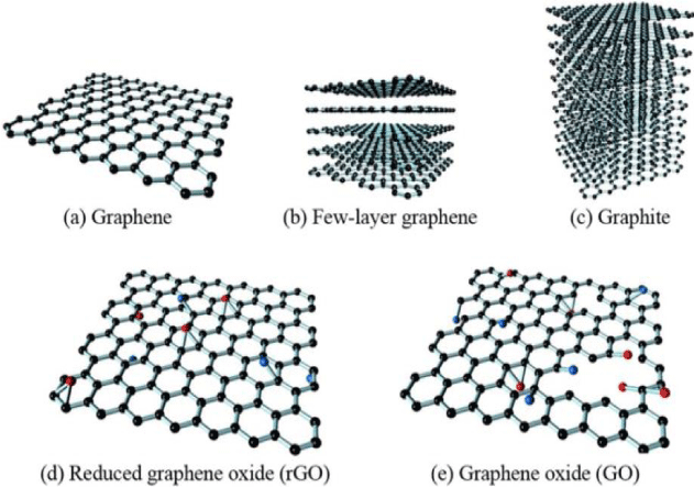
Figure 1:
Properties of graphene
Graphene exhibits exceptional mechanical and electronic properties. Its two-dimensional density is 0.763 mg/m², and it has a Young’s modulus of approximately 1 TPa (150 GPa or 150,000,000 psi). Graphene is the strongest material ever tested, with an intrinsic tensile strength of 130 GPa (19,000,000 psi). The engineering tensile strength for large-area, free-standing graphene ranges from 50 to 60 GPa. Due to its mechanical robustness, graphene mono layer can undergo large-angle bending with negligible strain, demonstrating the extraordinary resilience of this two-dimensional carbon nanostructure [3]. Even under extreme deformation, monolayer graphene retains its high charge carrier mobility.
Compared to bulk graphite, graphene has a stiffness of 0.5 TPa, and its spring constant ranges from 1 to 5 N/m. However, flat graphene sheets are thermodynamically unstable due to their high surface energy. For instance, when bent into a cylindrical shape—a configuration with lower energy—it tends to become unstable, leading to spontaneous scrolling.
Graphene in radiation shielding
Radiation shielding has long been a subject of scientific research, where key factors for material selection include cost, mass, size, and efficiency, rather than simply the ability to block radiation, as any material can act as a barrier to X-rays or gamma rays. Traditionally, materials such as concrete, copper, tin, and lead have been commonly used for radiation shielding.
Graphene, a unique allotrope of carbon, is classified among low-Z materials with weak intrinsic radiation absorption due to its low atomic number (Z = 6). This is expected, given that graphene consists of only a single atomic layer [4]. However, recent studies have demonstrated that multilayered graphene can serve as an effective radiation shield. In a graphene slab, which consists of tens of thousands of stacked single layers, the total thickness reaches approximately 10 μm.
Radiation is a significant concern for both human health and future technologies, making shielding an essential area of technological development. Graphene is now being considered a promising shielding material due to its low manufacturing cost, high absorption efficiency, and lightweight nature compared to conventional shielding materials. Additionally, graphene can be used in combination with boron (B), tungsten (W), and bismuth (Bi) to enhance its shielding capabilities.
Understanding topology in materials
Topology is the study of geometric properties that remain unchanged under continuous deformations such as stretching, twisting, or bending—provided that the structure is not cut or torn. A material exhibiting topological properties is of significant importance, as its electronic states remain robust against external perturbations.
Topological materials, particularly those with a single twisted configuration, can demonstrate robust quantum behavior, making them highly resistant to external disturbances. One notable consequence of topology in condensed matter physics is topological superconductivity, which is a state where electrical resistance completely vanishes at temperatures near absolute zero (0 K). In general, a superconductor is a material in which electrons form Cooper pairs at low temperatures, leading to zero electrical resistance, as described by the BCS theory [5].
Graphene, often referred to as a “wonder material,” continues to reveal novel quantum properties. Recent research has identified exotic topological quantum states in twisted bilayer graphene. A team of scientists has discovered that under specific conditions, electrons within graphene arrange themselves into topological electronic crystals, where they become “frozen” into a perfectly ordered pattern. Remarkably, despite being locked in place, the electrons exhibit synchronized spin motion, much like ballet dancers performing in unison.
This topological quantum behavior allows electric current to flow smoothly along the material’s edges while the interior remains non-conductive. This phenomenon is particularly relevant for energy-efficient electronic devices, quantum memory, and fault-tolerant quantum computing applications. By precisely twisting the graphene layers, researchers have engineered a unique electronic crystal state that facilitates edge conduction without resistance, providing new opportunities in quantum electronics.
The foundation of this discovery lies in layers of graphene, where two layers of carbon atoms are arranged in a honeycomb lattice (Figure 2). The hopping behavior of electrons between carbon atoms determines the material’s electronic properties, making it superficially similar to traditional conductors like copper but with fundamentally different quantum mechanical behavior.
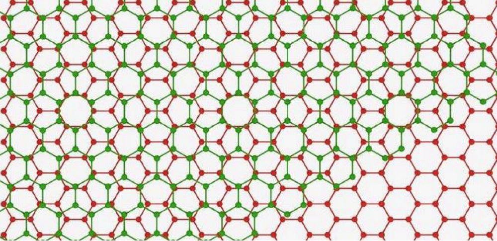
Figure 2: Twisted bilayer graphene near magic angle can adopt novel structural topology that facilitates faster electron mobility.
A fundamental example of topology is the Möbius strip, which represents a single 360-degree (Figure 3). In such a system, electrons can exist in spin-up or spin-down state [6].
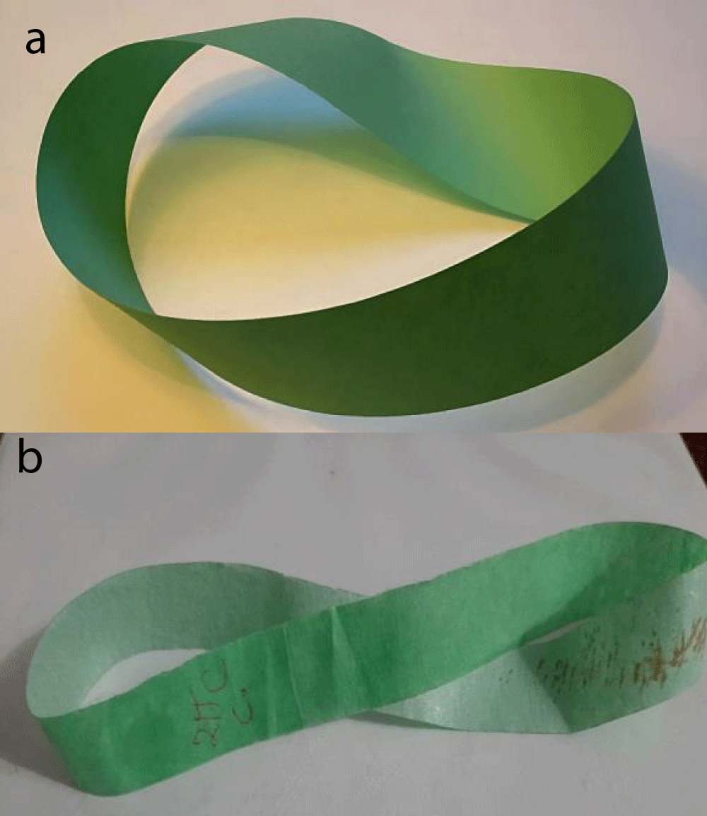
Figure 3: a) Möbius strip (Source: David Benbennick/Wikimedia Commons) b) 360-degree twisted strip of single layer graphene can give twisted and showing a near-Moiré topology at the magic angle (Figure 2).
The size distribution and topological properties of graphene samples in two-dimensional (2D) sheets have been investigated using several techniques, including X-ray diffraction (XRD) [7,8] and field-emission scanning electron microscopy (FE-SEM) [9,10] (Figure 4).

Figure 4: Electrochemical.
To determine the crystallite size, the Bragg equation (Eq. 1) and Scherrer equation (Eq.2) are used;
d = nλ/2sinθ (1)
Where d is the inter planar spacing (d-spacing), n is the diffraction order (n = 1, 2, 3,...), lambda [λ] is the wavelength of incident X-rays, and theta is the Bragg angle.
Bragg’s equation describes the condition for constructive interference when X-rays scatter off different atomic planes in a crystal (Figure 5).
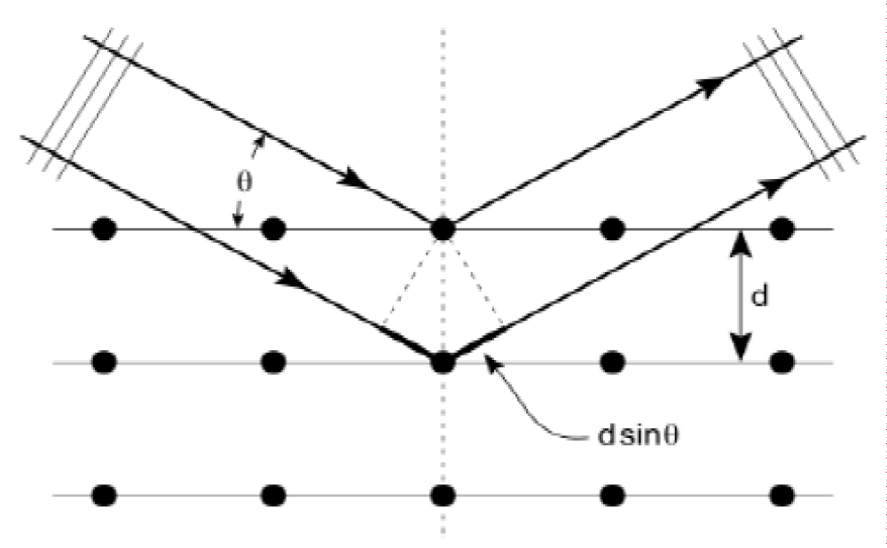
Figure 5: Two X-ray beams with identical wavelength (lambda [λ]) and phase coherence are scattered by different atoms. The lower X-ray beam travels an additional distance of (2dsin(theta). Constructive interference occurs when this extra path length is an integer multiple of the wavelength (lambda).
The Scherrer equation [11](Scherrer, P., 1918) is widely used in X-ray diffraction (XRD) and crystallography to determine crystallite size based on peak broadening in the diffraction pattern:(Eq. 2)
Ps = (λF) / B (2θ) cos θ. (2)
Where:
Ps is the average crystallite size, lambda is the X-ray wavelength, B(2\θ ) is the Full Width at Half Maximum (FWHM) of the diffraction peak, Theta is the Bragg angle, F is a shape factor, typically 1.0 for spherical particles and 1.1 for hexagonal graphene.
X-ray line broadening analysis provides an estimate of crystallite size, which often correlates well with values obtained from High-Resolution Transmission Electron Microscopy (HRTEM) shown in (Figure 6).
The FWHM is independent of the peak position (x = 0)) and remains invariant under transformation. The area within this FWHM (Eq. 3) range accounts for approximately 76% of the total peak area (Figure 6).
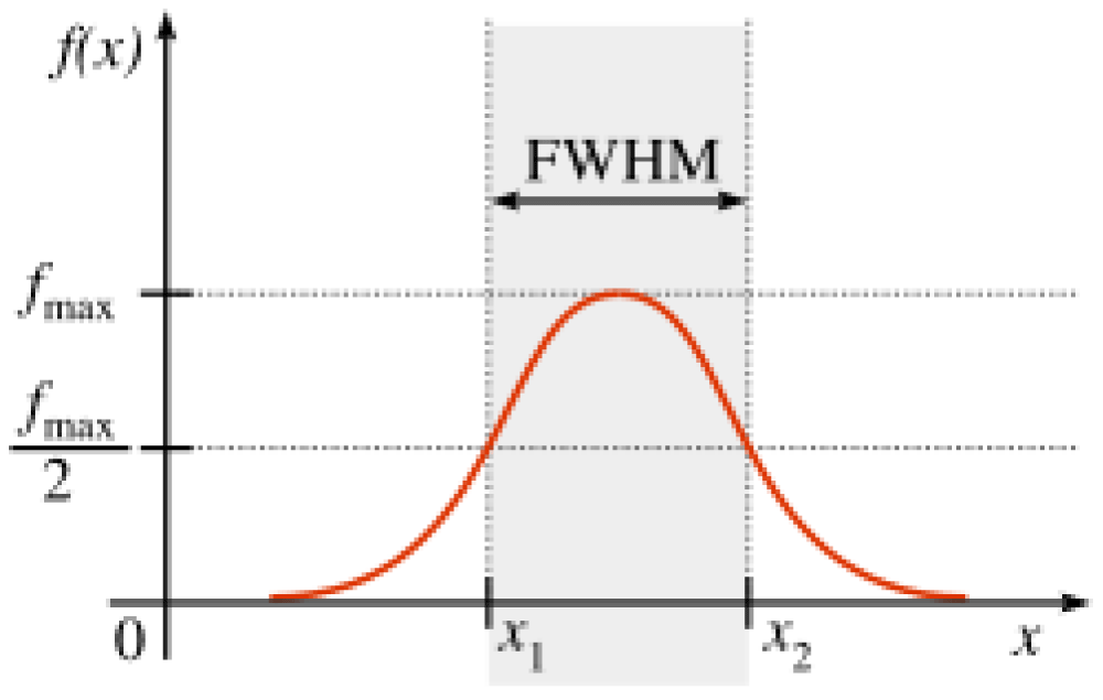
Figure 6: Full Width at Half Maximum (FWHM).
FWHM = 2√(2ln2)σ ≈ 2.355σ (3)
- Where σ is the standard deviation.
Using the XRD data, unique diffraction peak at different 2θ positions are selected for particle size distribution and topological characterization of graphene (Figures 7,8).
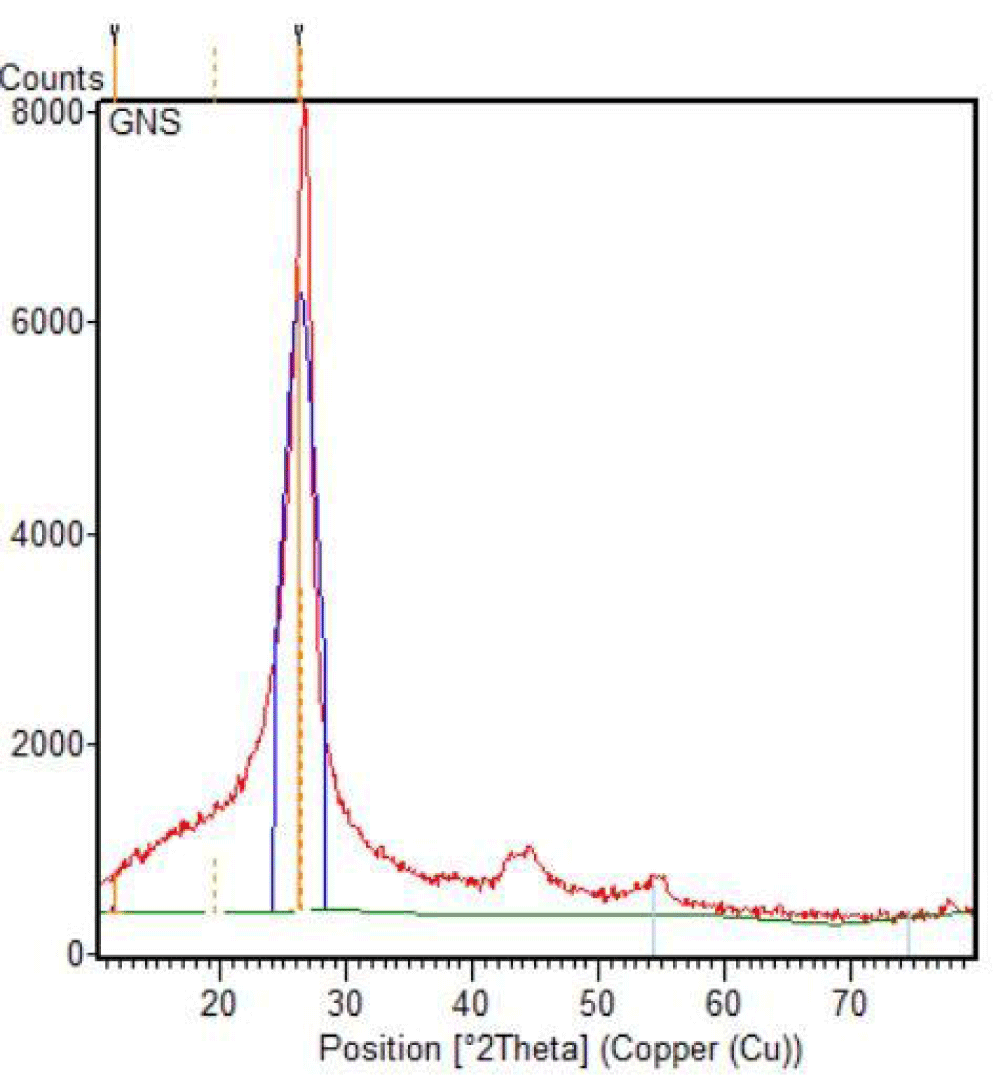
Figure 7: XRD spectrum of graphene with phase matching.
Figure 8: Captopril.
Using the XRD data, unique diffraction peaks at different 2θ positions are selected for particle size distribution and topological characterization of graphene-based materials, which crystallized graphene components (81%) and amorphous graphene components (19%), characterized via XRD data (Table 1 and Figures 9,10).
| Table 1: Particle size distribution for the graphene sample components. | |||||||
| NO. | Components λ=0.15406nm |
2θ Angle |
d-spacing (nm) | FWHM (2θ) |
Shape Factor SF |
Particle Size (nm) PS | Size% |
| 1 | GO. | 11.543 | 0.766162 | 0.0900 | 1.00 | 98.08. | 11.54 |
| 2 | PRGO. | 19.449 | 0.456257 | 4.0000 | 0.94 | 2.10 | 22.21 |
| 3 | GNs. | 26.250 | 0.339225 | 3.4428 | 1.10 | 2.82 | 66.25 |
| Average | Asf = 1.03 | Aps = 34.33 | 100% | ||||
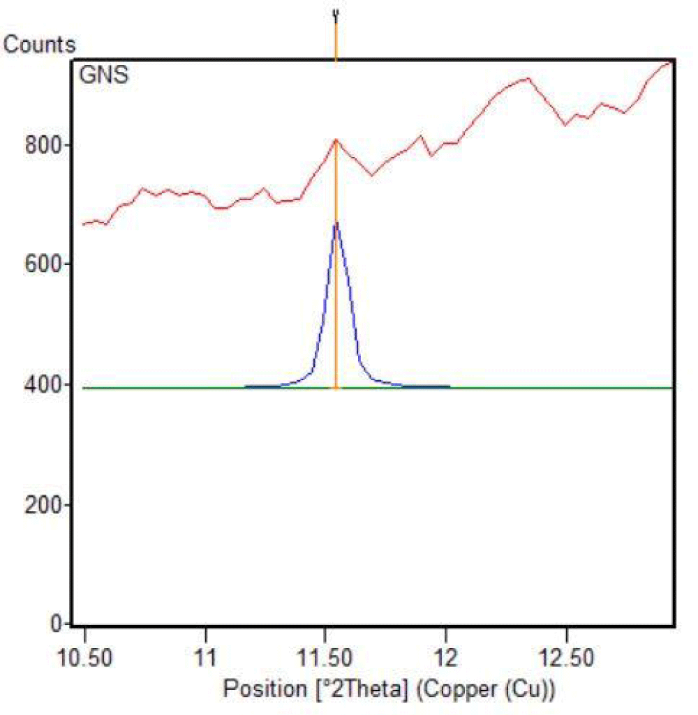
Figure 9: Graphene oxide (GO) phase matched with XRD spectrum.
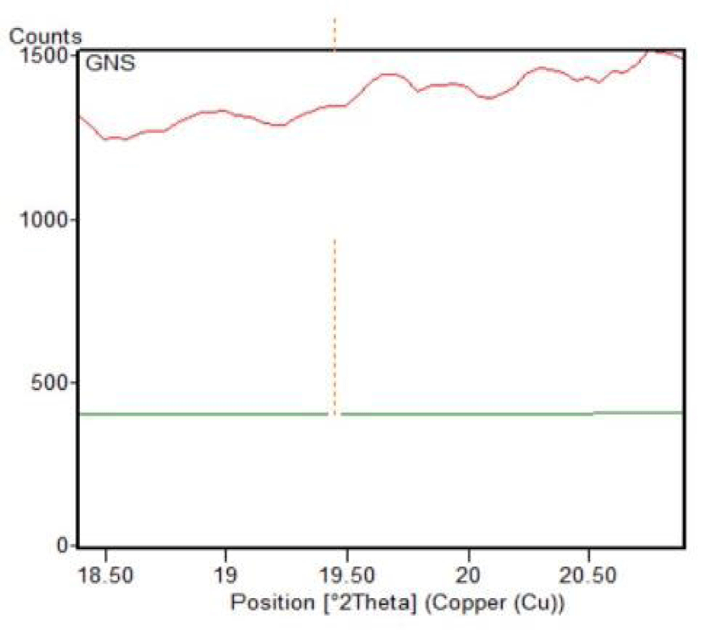
Figure 10: Partially reduced graphene oxide (PRGO) phase matched with XRD spectrum.
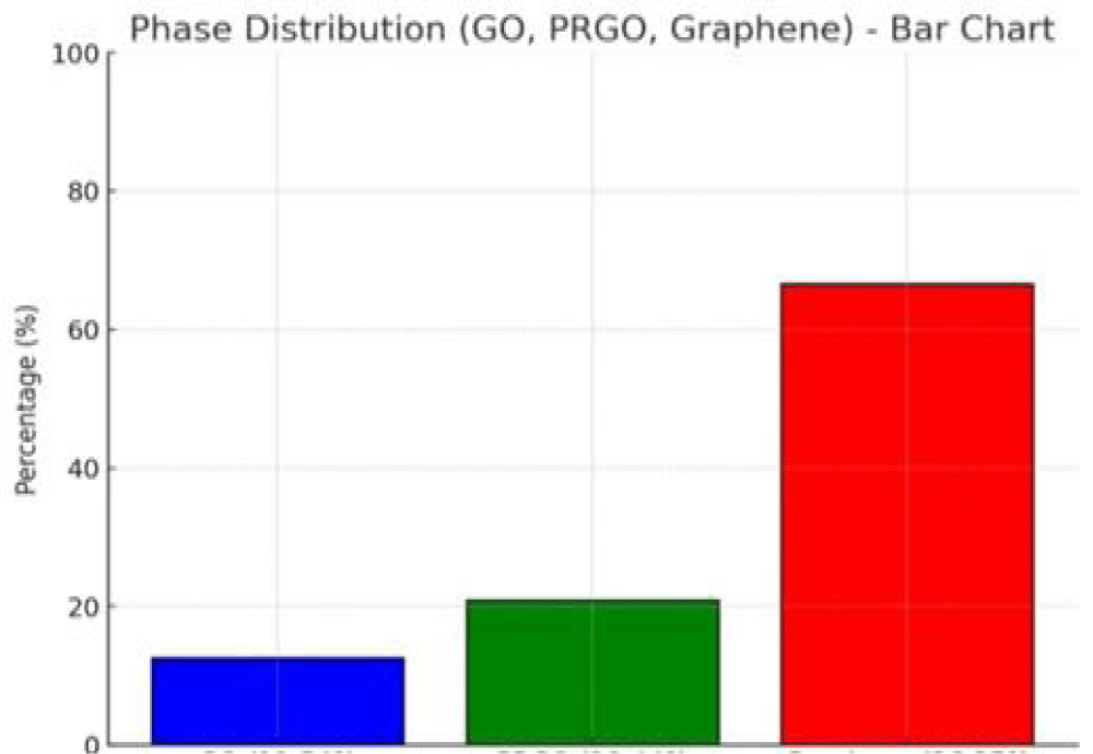
Figure 11: Phase diagram showing intensity distribution of the graphene sample components. Blue bar Go = 11.54%, green bar PRGO = 22.21% and red bar Graphene = 66.25%
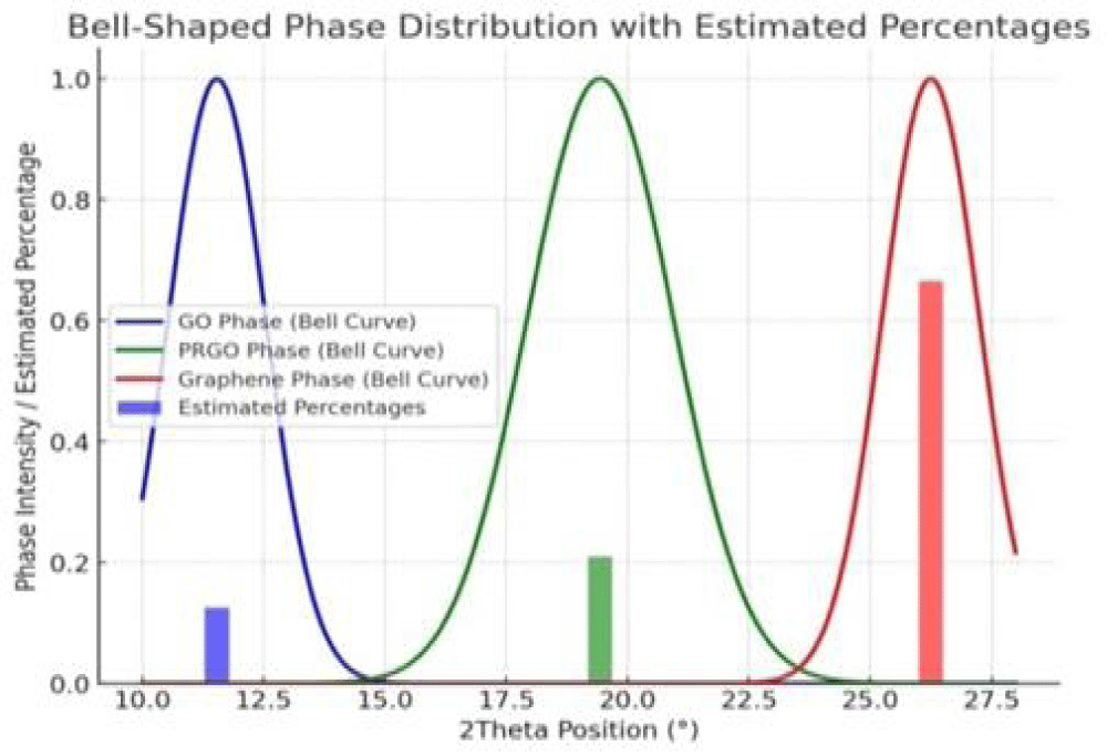
Figure 12: Normalized phase intensity distribution based on 2θ values.
Raman spectroscopy
Raman spectroscopy is a powerful technique for the qualitative analysis of graphene, allowing determination of single-layer, bilayer, and multilayer graphene based on peak position, intensity, and broadening. The Raman shift spectrum of the graphene sample is presented in Figure 13.
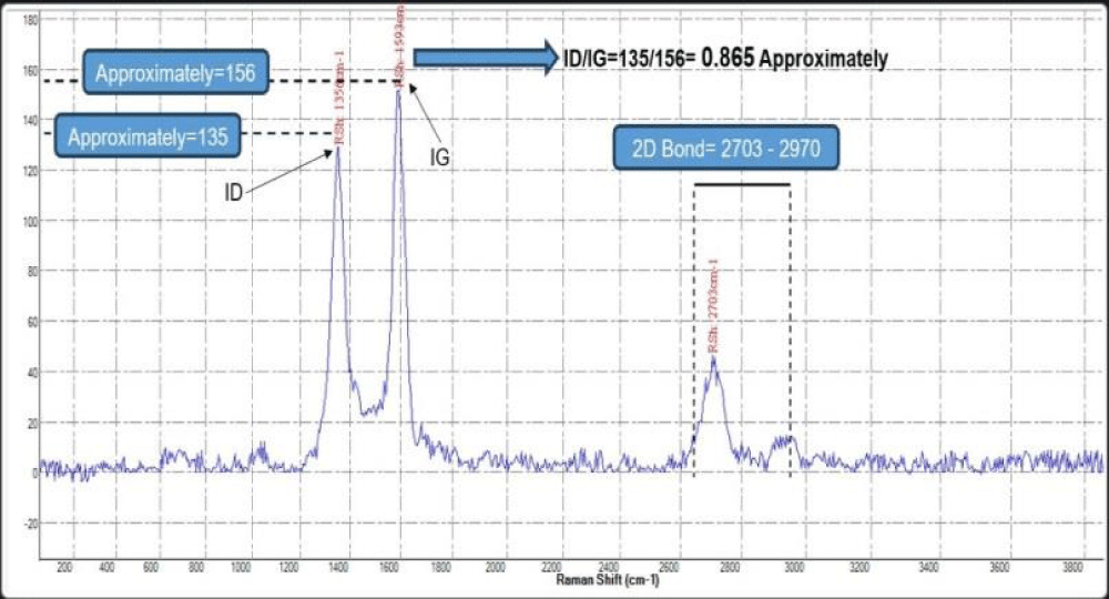
Figure 13: Raman shift spectrum of the graphene sample.
Raman spectral ratios for the graphene characterization:
ID/IG = 135/156 = 0.879 (indicating multilayer graphene)
I2D/IG = 44/156 = 0.282 (confirming multilayer graphene)
FE-SEM imaging and FT-IR particle size analysis
Scanning Electron Microscopy (SEM) provides insights into the morphology and size distribution of graphene samples at different magnifications. Figures 14,15 display SEM images of graphene in different configurations.
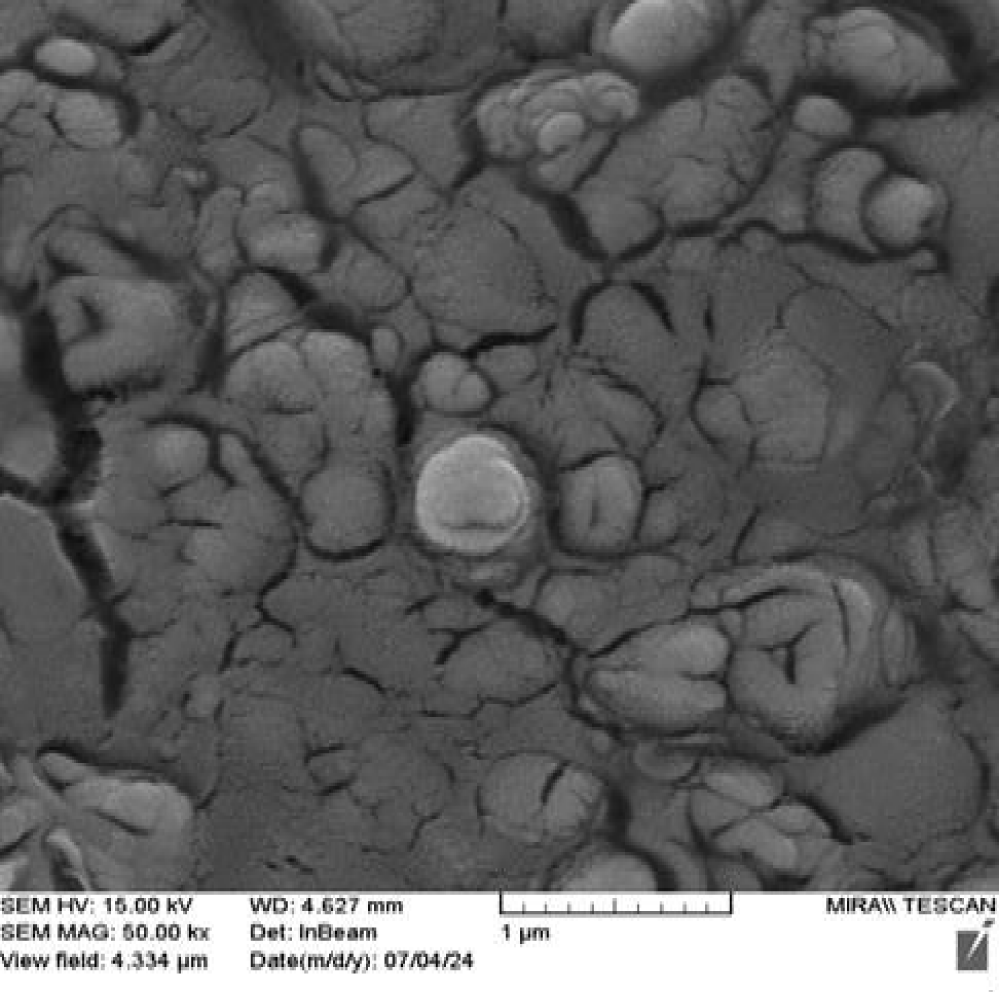
Figure 14: FE-SEM image for the sample in 1 Micrometer scale.
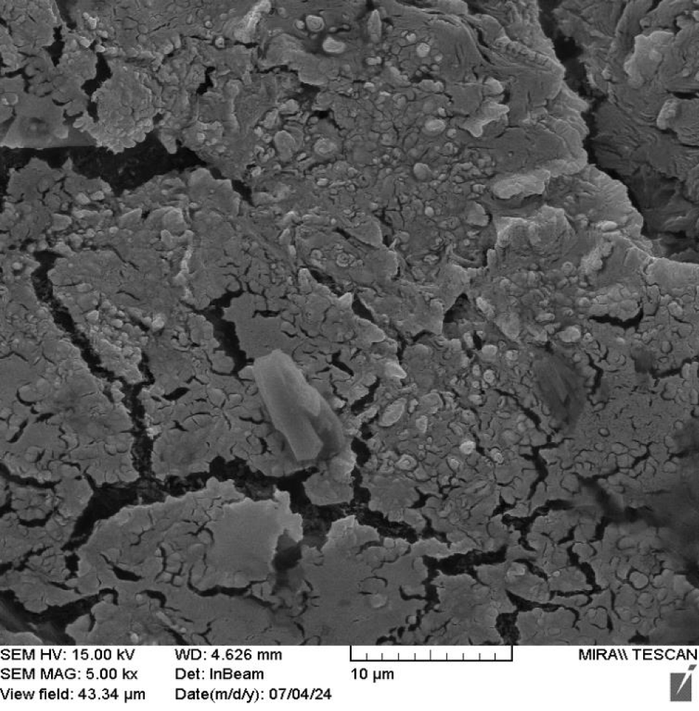
Figure 15: Graphene components in various forms observed through FE-SEM.
Rippling is a crucial properties of 2D graphene sheets and can be seen on those images. Understanding the relationship between rippling and defects is essential for technologies such as flexible electronics, catalysis and energy storage. Graphene crystallite structure in Figure 14 twisted and folded as multilayer graphene, consistent with the Raman spectrum (Figure 13).
The Fourier Transform Infrared (FT-IR) spectrum of the sample is presented in Figure 16, illustrating the absorption peaks corresponding to various functional groups. The spectrum is divided into two regions: the fingerprint region (400 - 1500 cm⁻¹) and the functional group region (1500 - 4000 cm⁻¹). The peak at 3417.70 cm⁻¹ corresponds with a lower intensity peak indicating the hydroxyl (-OH) group compared to graphene components. Additionally, the peak at 1624.02 cm⁻¹ corresponds to the carbonyl (C = O) functional group, which is more pronounced in graphene components. The graphene structures identified in the XRD spectrum (Figures 7-12) are primarily associated with the functional group region (1624.02 - 3417.7 cm⁻¹).
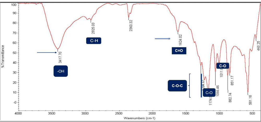
Figure 16: FT-IR spectrum of the graphene sample showing impurities.
UV-Vis analysis of the sample
The UV-Visible spectrum of the sample is depicted in Figure 17, highlighting the characteristic absorption peaks of graphene and its derivatives. The absorption peaks are observed at:
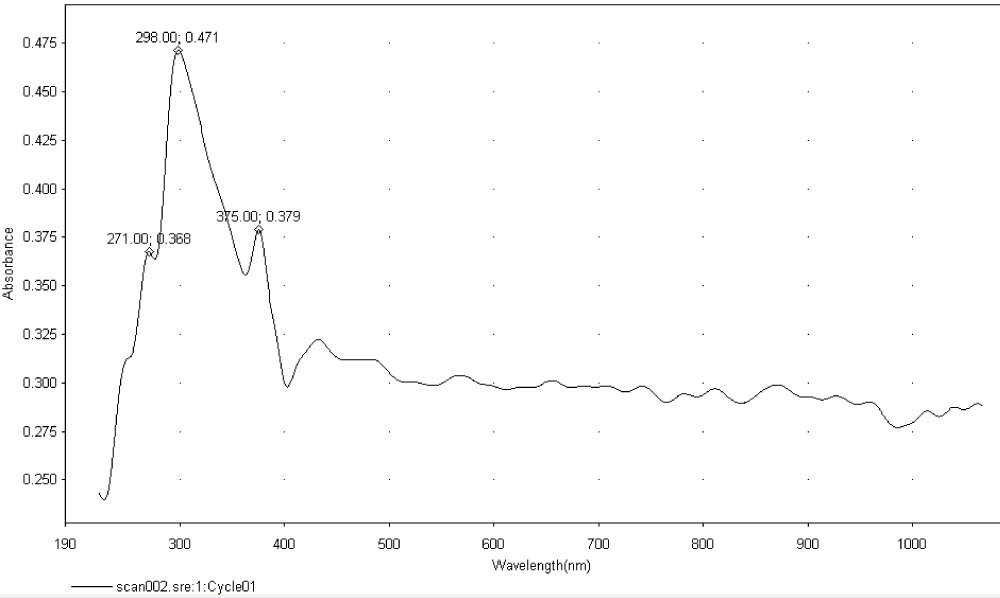
Figure 17: UV-Vis spectrum of the sample (GO: 238 nm, Graphene: 271 nm, RGO: 298 nm, PRGO: 375 nm).
238 nm (Graphene Oxide, GO)
271 nm (Graphene)
298 nm ((Partially Reduced Graphene Oxide, PRGO)
The estimated band gap energy of graphene, determined using the Tauc plot (derived from the UV-Vis spectrum in Figure 18), provides insights into the electronic properties of the graphene components.
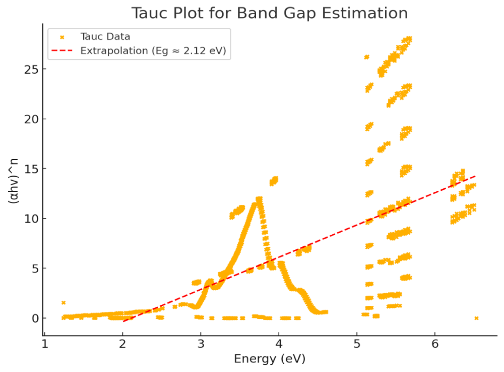
Figure 18: Tauc plot for determination of the band gap energy.
The Tauc plot, used for estimating the optical band gap, is governed by the following equation (Eq. 4):
(𝛼·ℎ𝜈)n = A(ℎ𝜈−𝐸g) (4)
where:
h is Planck’s constant,
‘𝜈’ is photon frequency,
Eg is the band gap energy, and
A is a proportionality constant (related to slope)
The value of n varies based on the type of electronic transition (direct or indirect), where n = 1/γ, with γ being a factor dependent on the nature of the electronic transition. For direct and indirect transitions, γ is 1/2 and 2, respectively [12]. The band gap energy is generally determined using diffuse reflectance spectra [13-15].
For multilayer graphene, the absorption coefficient (𝛼) is related to the scattering coefficient (s) as (𝛼 = k/s), where k represents the absorption coefficient. Based on the Tauc plot (Figure 18), the estimated band gap values for different graphene structures are as follows:
Graphene crystalline (GNs): ~2.12 eV
Partially reduced graphene oxide (PRGO): 0.3 - 1.5 eV
Graphene Oxide (GO): 2.1 - 3.5 eV
A comparison of band gap energy values for different graphene components is presented in Table 2.
| Table 2: Band gap energy of the grapheme components. | |
| Components | Band Gap Energy (eV) |
| Graphene Oxide (GO) | ~2.1 - 3.5 eV |
| Partially reduced graphene oxide (PRGO) | ~0.3 - 1.5 eV |
| Graphene (GNs) | ~2.12 eV |
Based on peak analysis (Figure 7) and calculations from spectral and imaging data, the graphene sample exhibits a multilayer topology.
- The average particle size of graphene components is 34.33 nm, placing it well within the nano-particle size range (Table 1).
- The twisted topology observed in the sample (Figure 14) suggests potential applications in superconductivity.
- Impurities introduced during the synthesis of graphene sample can be minimized through optimized drying techniques (Figure 16).
- The proposed twisted graphene sheet topology (Figure 3) can facilitate electron spin polarization, enabling applications in quantum materials.
- Band gap energy values were determined using Tauc plots (Figure 18) and summarized in Table 2.
- GO exhibits a higher band gap (2.1 – 3.5 eV) which interrupt the π-conjugated electron network and increase the band gap.
- PRGO has a lower band gap (0.3 – 1.5 eV), as reduction removes some oxygen groups, partially restoring electrical conductivity.
- Graphene (~2.12 eV) demonstrates a moderate band gap, suggesting that it may exhibit partial reduction or an intermediate superconducting state due to its unique topological characteristics.
This study highlights the topological properties, size distribution, and structural characterization of graphene using advanced techniques such as XRD, FE-SEM, and Raman spectroscopy. The results demonstrate that graphene’s unique electronic structure and mechanical robustness make it a promising material for various technological applications, including quantum computing, superconductivity, and radiation shielding.
The authors gratefully acknowledge Azam Pourentazari and Roya Boca who have worked on the computer codes used in this work. Funds for this research were provided by the PGPZ International and Beamgostar Lab.
- Foroutan T, Nazemi N, Tavana M, Kassaee MZ, Motamedi E, Sonieshargh S, et al. Suspended graphene oxide nano particle for accelerate multilayer osteoblast attachment. J Biomed Mater Res A. 2018;106(1):293–303. Available from: https://onlinelibrary.wiley.com/doi/abs/10.1002/jbm.a.36231
- Motamedi E, Talebi Atouei M, Kassaee MZ. Comparison of nitrate removal from water via graphene oxide coated Fe, Ni and Co nano-particles. Mater Res Bull. 2014;54:34–40. Available from: https://doi.org/10.1016/j.materresbull.2014.02.019
- Zhang Y. Comprehensive review on the mechanical properties of graphene. Mater Today. 2020;33:24–34.
- Wang L. Particle size distribution in graphene and its effect on material properties. Graphene Technol. 2023;8(1):112–20.
- Bardeen J, Cooper LN, Schrieffer JR. Theory of superconductivity. Phys Rev. 1957;108(5):1175–204. Available from: https://journals.aps.org/pr/abstract/10.1103/PhysRev.108.1175
- Chen X. Synthesis and structural analysis of graphene micro-particles. J Nanomater. 2022;23(5):948–56.
- Lee C. Phase identification in graphene samples using X-ray diffraction. Mater Sci Eng. 2019;66(8):1820–7.
- Jiang F. XRD patterns in graphene: a tool for crystallographic studies. Cryst Growth Des. 2023;23(2):456–65.
- Kim D. FE-SEM analysis of graphene for high-resolution imaging. Nano Res. 2021;14(3):789–98.
- Patel S. Advances in imaging and analysis techniques for graphene micro-particles using FE-SEM. Microsc Microanal. 2022;28(4):540–55.
- Scherrer P. GottingenNachrichten, Math Phys. 1918;2:98–100. Available from: https://www.scirp.org/reference/referencespapers?referenceid=1931994
- Pankove J. Optical processes in semiconductors. New York: Courier Corporation. 1971.
- Kubelka P, Munk F. Contribution to the optics of pigments. Z Tech Phys. 1931;12:593–9.
- Sepehri A, Ghassem-Alaskari MK. The feasibility of synthesized micro graphene particles. 9th International Conference on Researches in Science & Engineering; 2025; Bangkok, Thailand. EN-P-543.
- Smith J. Electrical properties of graphene micro-particles. J Adv Mater. 2020;58(12):2349–56.